
onsemi MC74HC04ADTR2G Hex Inverter: Datasheet, Pinout, and Application Circuit Guide
The MC74HC04ADTR2G from onsemi is a high-performance, high-speed CMOS logic device belonging to the ubiquitous 74HC series. It integrates six independent inverting buffers, also known as NOT gates, into a single compact package. This IC is designed to operate with a wide power supply range, typically from 2.0V to 6.0V, making it compatible with various logic levels, including 3.3V and 5V systems. Its high noise immunity and low power consumption are hallmarks of the HC family, making it a fundamental component in countless digital circuits.
Datasheet Overview: Key Specifications
A thorough review of the datasheet is essential for proper implementation. Key absolute maximum ratings include a supply voltage (VCC) range of -0.5V to +7.0V and an input voltage range of -0.5V to VCC + 0.5V. Staying within these limits is critical to prevent permanent device damage.
Under recommended operating conditions, the device showcases its core performance:
High-Speed Operation: Typical propagation delay times of 13 ns at 4.5V VCC.
Low Power Consumption: Very low static power dissipation, with a maximum ICC of 20 µA.
High Output Current: Capable of sourcing or sinking up to 4 mA at the output pins.
Wide Operating Temperature Range: From -55°C to +125°C, suitable for industrial and automotive applications.
Pinout Configuration
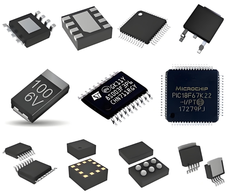
The "DTR2G" suffix denotes a TSSOP-14 package, which is surface-mount and space-efficient. The pinout is standard for a Hex Inverter:
Pins 1, 3, 5, 9, 11, 13 (Inputs): The inputs to the six individual inverters (1A through 6A).
Pins 2, 4, 6, 8, 10, 12 (Outputs): The corresponding outputs (1Y through 6Y). Each output is the logical complement of its input.
Pin 7 (GND): Ground reference (0V).
Pin 14 (VCC): Positive power supply pin (2V to 6V).
Application Circuit Guide
The primary function of an inverter is to provide logic level inversion. A simple application involves connecting a digital signal (e.g., from a microcontroller GPIO) to an input pin; the output will be the exact opposite state.
Beyond simple inversion, the MC74HC04ADTR2G is incredibly versatile:
1. Crystal Oscillator Circuit: A fundamental application is building a simple crystal oscillator. Two inverters are used: one is connected in a feedback loop with a crystal resonator (e.g., 4 MHz or 8 MHz) and load capacitors between its input and output. The second inverter buffers the generated clock signal for use by other ICs like microcontrollers.
2. Waveform Shaping/Schmitt Trigger: While not a true Schmitt trigger input, a standard inverter with positive feedback (a resistor connected from output to input) can be used to square up noisy or slow-rise-time signals, providing hysteresis and cleaner digital transitions.
3. Driving Loads: The IC can be used as a simple buffer to drive higher-current loads like LEDs or small relays. A current-limiting resistor is essential when driving an LED directly from the output pin.
4. Creating Basic Logic Gates: By combining multiple inverters with other gates (e.g., AND, OR), more complex functions can be built. For instance, an inverter is used to create a NAND gate from an AND gate's output.
The onsemi MC74HC04ADTR2G stands as a quintessential component in digital design. Its robust performance, wide voltage compatibility, and multi-functionality—from simple signal inversion and clock generation to waveform conditioning—make it an indispensable tool for engineers and hobbyists alike. Its availability in a space-saving TSSOP package further ensures its relevance in modern, compact electronic designs.
Keywords: Hex Inverter, CMOS Logic, MC74HC04ADTR2G, Crystal Oscillator, Waveform Shaping

